Schematic-driven development
Boards that start clean, stay constraint-driven, and survive review.
- Schematic capture & netlist-driven design
- Engineering constraints & change notes
- Component selection and BOM groundwork
Schematic-driven development, high-speed layout, controlled-impedance routing, and fabrication-ready documentation for embedded systems, electronics products, and custom hardware.
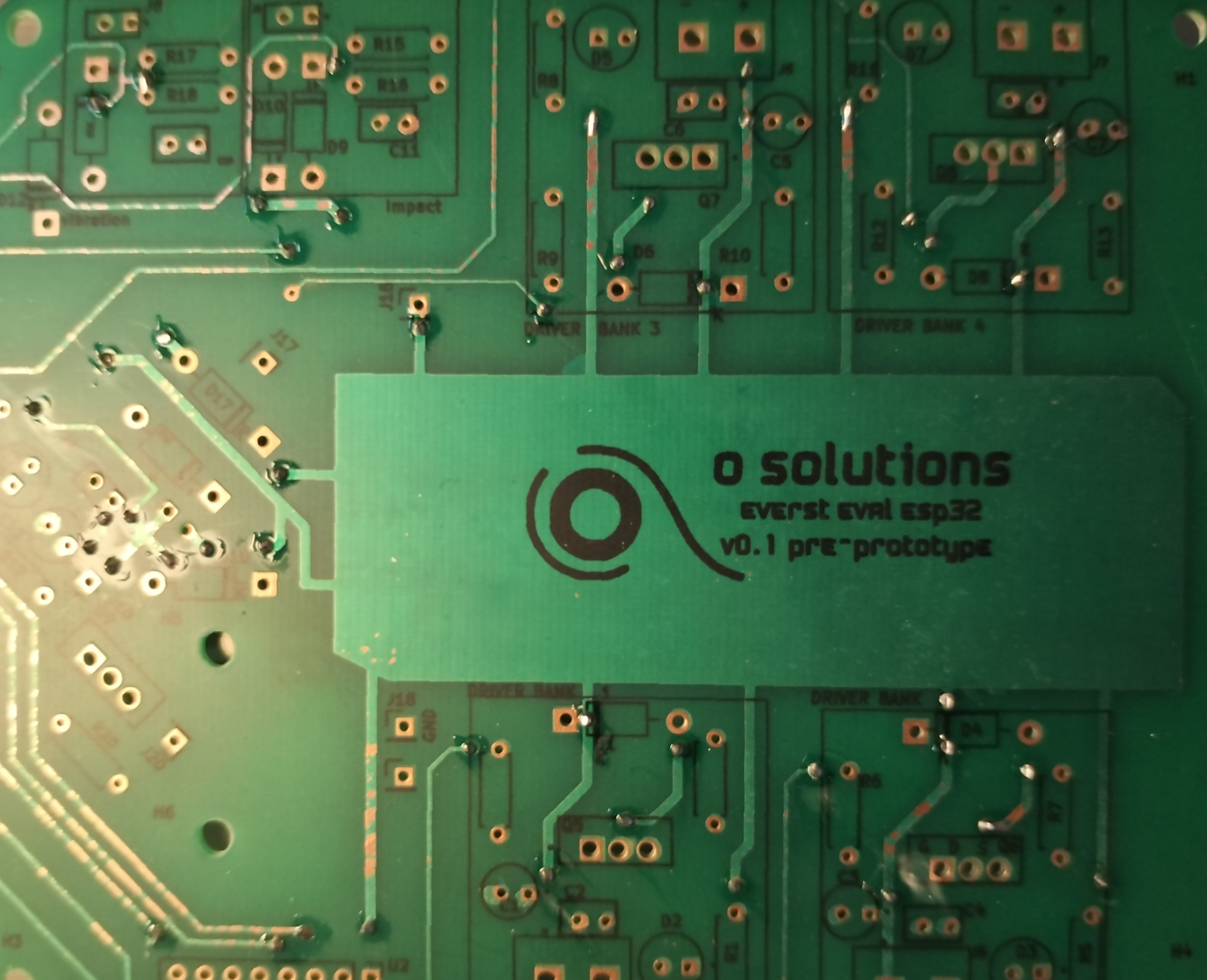
PCB design and engineering delivered around your embedded system, electronics product, or custom hardware — from schematic through fabrication-ready outputs and into the mechanical enclosure.
Boards that start clean, stay constraint-driven, and survive review.
Multi-layer PCB design with deliberate placement and routing.
Design with the factory and the assembly line in mind from day one.
From dense mixed-signal boards to power stages that stay cool.
Fast interfaces designed with electrical reality in mind.
Documentation a fab and a pick-and-place can act on without guessing.
High-speed PCBs are becoming increasingly commonplace, and high-performance design and manufacturing are quickly becoming the industry standard.
High-speed PCB design requires careful consideration of more than just routing. Controlled-impedance nets, clean return paths, and disciplined stack-ups all have to line up — and the requirements have to survive the hand-off to fabrication without ambiguity.
We plan impedance requirements early, design controlled-impedance traces to a target, and specify those requirements directly in the fabrication documentation. Work proceeds from the manufacturer's recommended stack-up, with capability verified up front so the fab can actually meet the electrical and fabrication demands of the design.
PCB designs can be prepared to support applicable manufacturing and compliance requirements when requested. The reference list below reflects the kinds of quality and compliance programs common across fabrication partners.
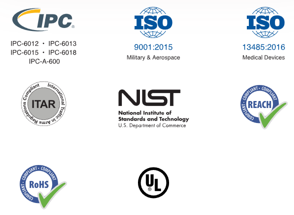
When requested, the design, documentation, and output package are prepared so a qualified fabrication partner can build against the applicable manufacturing and quality programs — standards such as IPC-6012, IPC-6013, IPC-6015, IPC-6018 and IPC-A-600 for board quality and workmanship, ISO 9001:2015 and ISO 13485:2016 for quality management, and programs such as ITAR, NIST, REACH, RoHS, and UL where relevant to the product.
O Solutions Technologies does not claim to hold these registrations itself. These are manufacturing-side requirements — we keep them in view during design so the deliverables can support them when requested, rather than assuming every project targets them.
If your application must meet a specific standard, mention it in the inquiry — the design scope and documentation plan will be set up around it from the start.
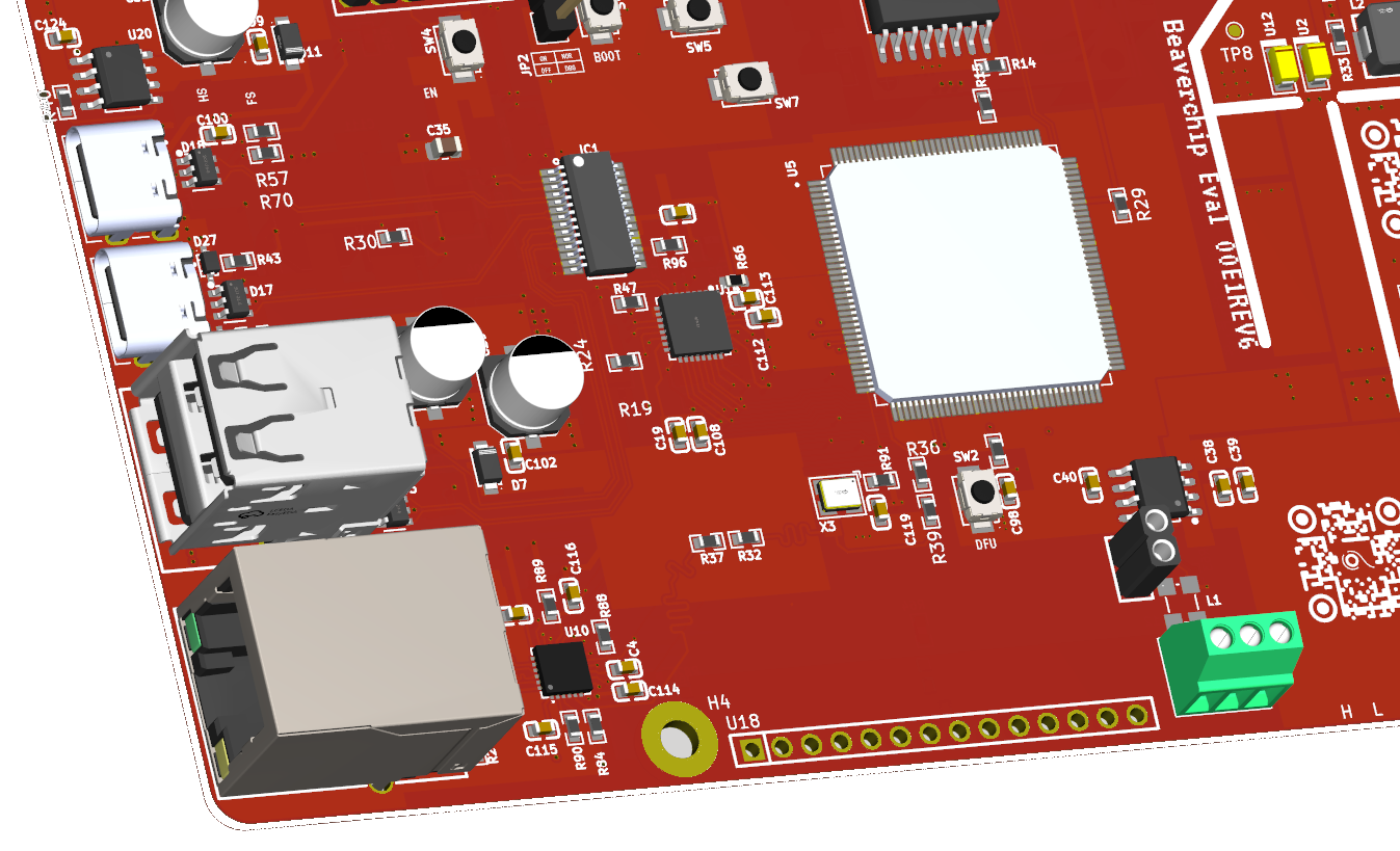
PCB renders
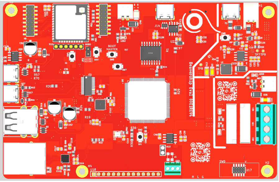
Schematic-driven digital/analog layout with clean power and IO partitioning.
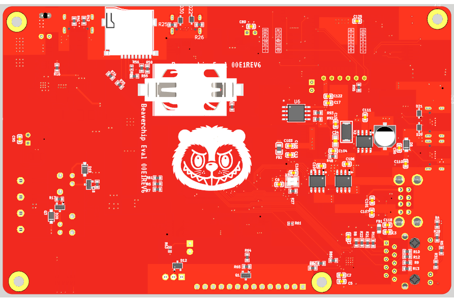
Controlled-impedance routing on differential pairs, built around the target stack-up.
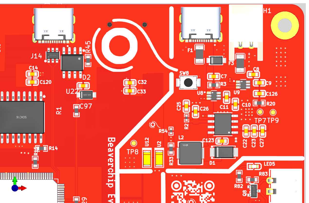
Current-focused layout with deliberate copper, thermal, and mounting planning.
.png)
PCB development can be complemented by enclosure and mechanical design. A board that fits its product on the first try saves an entire prototyping cycle — so mechanical integration is treated as part of the engineering scope, not an afterthought.
.png)
.png)
.png)
.png)
.png)
.png)
Share whatever you know — only name and email are required. Design scope, layer counts, and quantities can be refined together once the project starts.
Reach engineering directly, or message O Solutions Technologies on WhatsApp with your board requirements.